User Guide
Page 14
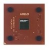
..., SSE and 3DNow! Figure 1 on Socket A. technology. The AMD Athlon XP processor model 6 with QuantiSpeed architecture incorporates three TLB optimizations: the L1 DTLB increases from 32 to 40 entries, the L2 ITLB and L2 DTLB both enhanced data and instruction address translation. The AMD Athlon XP processor model 6 delivers excellent system performance in the AMD Athlon XP processor model 6 includes new integer multimedia...
..., SSE and 3DNow! Figure 1 on Socket A. technology. The AMD Athlon XP processor model 6 with QuantiSpeed architecture incorporates three TLB optimizations: the L1 DTLB increases from 32 to 40 entries, the L2 ITLB and L2 DTLB both enhanced data and instruction address translation. The AMD Athlon XP processor model 6 delivers excellent system performance in the AMD Athlon XP processor model 6 includes new integer multimedia...

User Guide
Page 17
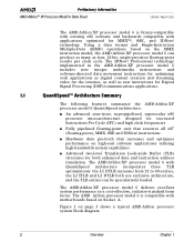
... 51. The signal inputs use an impedance controlled push-pull, low-voltage, swing-signaling technology contained within the Socket A socket. 24309E-March 2002 Preliminary Information AMD Athlon™ XP Processor Model 6 Data Sheet 2 Interface Signals 2.1 Overview The AMD Athlon™ system bus architecture is designed to bring the signal past the input threshold. The interface signals use differential...
... 51. The signal inputs use an impedance controlled push-pull, low-voltage, swing-signaling technology contained within the Socket A socket. 24309E-March 2002 Preliminary Information AMD Athlon™ XP Processor Model 6 Data Sheet 2 Interface Signals 2.1 Overview The AMD Athlon™ system bus architecture is designed to bring the signal past the input threshold. The interface signals use differential...
User Guide
Page 59
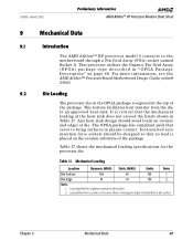
...socket named Socket A. It is placed on page 48. This processor utilizes the Organic Pin Grid Array (OPGA) package type described in Table 17. The OPGA package has compliant pads that the mechanical loading of inclination to die surface. 2. Chapter 9 Mechanical Data 47 24309E-March 2002 Preliminary Information AMD Athlon™ XP Processor... Model 6 Data Sheet 9 Mechanical Data 9.1 Introduction The AMD Athlon™ XP processor model 6 connects to an approved heat sink. ...
...socket named Socket A. It is placed on page 48. This processor utilizes the Organic Pin Grid Array (OPGA) package type described in Table 17. The OPGA package has compliant pads that the mechanical loading of inclination to die surface. 2. Chapter 9 Mechanical Data 47 24309E-March 2002 Preliminary Information AMD Athlon™ XP Processor... Model 6 Data Sheet 9 Mechanical Data 9.1 Introduction The AMD Athlon™ XP processor model 6 connects to an approved heat sink. ...

User Guide
Page 72
... B28 VCC_CORE A29 SDATA[44]# P B G B30 VSS A31 NC Pin page 72 - - - Preliminary Information AMD Athlon™ XP Processor Model 6 Data Sheet 24309E-March 2002 10.2 Pin List Table 20 cross-references Socket A pin location to the current return paths. The "L" (Level) column shows the electrical specification for the purpose ...VCC_CORE A5 SADDOUT[5]# P O G B6 VSS A7 SADDOUT[3]# P O G B8 VCC_CORE A9 SDATA[55]# P B P B10 VSS A11 SDATA[61]# P B P B12 VCC_CORE A13 SDATA[53]# P B G B14 VSS A15 SDATA[63]# P B G B16 VCC_CORE A17 SDATA[62]# P B G B18 VSS A19 NC Pin page 72 - - -
... B28 VCC_CORE A29 SDATA[44]# P B G B30 VSS A31 NC Pin page 72 - - - Preliminary Information AMD Athlon™ XP Processor Model 6 Data Sheet 24309E-March 2002 10.2 Pin List Table 20 cross-references Socket A pin location to the current return paths. The "L" (Level) column shows the electrical specification for the purpose ...VCC_CORE A5 SADDOUT[5]# P O G B6 VSS A7 SADDOUT[3]# P O G B8 VCC_CORE A9 SDATA[55]# P B P B10 VSS A11 SDATA[61]# P B P B12 VCC_CORE A13 SDATA[53]# P B G B14 VSS A15 SDATA[63]# P B G B16 VCC_CORE A17 SDATA[62]# P B G B18 VSS A19 NC Pin page 72 - - -
User Guide
Page 80
... input. Preliminary Information AMD Athlon™ XP Processor Model 6 Data Sheet 24309E-March 2002 10.3 Detailed Pin Descriptions A20M# Pin The information in this section pertains to simulate address wrap-around in the 20-bit 8086. A20M# is a feature that blocks this pin location. AMD Pin AMD Athlon™ System Bus Pins Analog Pin AMD Socket A processors do not implement...
... input. Preliminary Information AMD Athlon™ XP Processor Model 6 Data Sheet 24309E-March 2002 10.3 Detailed Pin Descriptions A20M# Pin The information in this section pertains to simulate address wrap-around in the 20-bit 8086. A20M# is a feature that blocks this pin location. AMD Pin AMD Athlon™ System Bus Pins Analog Pin AMD Socket A processors do not implement...

User Guide
Page 81
24309E-March 2002 Preliminary Information AMD Athlon™ XP Processor Model 6 Data Sheet CONNECT Pin COREFB and COREFB# Pins CPU_PRESENCE# Pin DBRDY and DBREQ# Pins FERR Pin See "SYSCLK and SYSCLK#" on page 73 for ... or absence of the NE bit in the Socket A-style socket. FERR is an input from the system used to VSS on the motherboard, CPU_PRESENCE# may be inverted and level shifted to the system that is asserted for any unmasked numerical exception independent of a processor in CR0. Chapter 10 Pin Descriptions 69 CONNECT...
24309E-March 2002 Preliminary Information AMD Athlon™ XP Processor Model 6 Data Sheet CONNECT Pin COREFB and COREFB# Pins CPU_PRESENCE# Pin DBRDY and DBREQ# Pins FERR Pin See "SYSCLK and SYSCLK#" on page 73 for ... or absence of the NE bit in the Socket A-style socket. FERR is an input from the system used to VSS on the motherboard, CPU_PRESENCE# may be inverted and level shifted to the system that is asserted for any unmasked numerical exception independent of a processor in CR0. Chapter 10 Pin Descriptions 69 CONNECT...
User Guide
Page 83
... 2.5 V tolerant. For information about the FID[3:0] isolation circuit, see the AMD Athlon™ Processor-Based Motherboard Design Guide, order# 24363. FLUSH# must always provide for pins at 0_FFFF_FFF0h. However, sockets that allows PGA key pins only where designated. These 16 locations are 50 ohms...AG15, AG17, AG27, and AG29). 24309E-March 2002 Preliminary Information AMD Athlon™ XP Processor Model 6 Data Sheet FLUSH# Pin IGNNE# Pin INIT# Pin INTR Pin JTAG Pins K7CLKOUT and K7CLKOUT# Pins Key Pins The processor FID[3:0] outputs are each run for two to three inches and ...
... 2.5 V tolerant. For information about the FID[3:0] isolation circuit, see the AMD Athlon™ Processor-Based Motherboard Design Guide, order# 24363. FLUSH# must always provide for pins at 0_FFFF_FFF0h. However, sockets that allows PGA key pins only where designated. These 16 locations are 50 ohms...AG15, AG17, AG27, and AG29). 24309E-March 2002 Preliminary Information AMD Athlon™ XP Processor Model 6 Data Sheet FLUSH# Pin IGNNE# Pin INIT# Pin INTR Pin JTAG Pins K7CLKOUT and K7CLKOUT# Pins Key Pins The processor FID[3:0] outputs are each run for two to three inches and ...

User Guide
Page 84
...pulldown resistors to ground on page 43. The AMD Athlon XP processor model 6 does not support SADDIN[1:0]# or SADDOUT[1:0]#. This interface is an input from the system that causes a non-maskable interrupt. Preliminary Information AMD Athlon™ XP Processor Model 6 Data Sheet 24309E-March 2002 NC ...Pins NMI Pin PGA Orientation Pins PLL Bypass and Test Pins PWROK Pin SADDIN[1:0]# and SADDOUT[1:0]# Pins Scan Pins See "NC Pins" for a PGA socket pin at pin locations ...
...pulldown resistors to ground on page 43. The AMD Athlon XP processor model 6 does not support SADDIN[1:0]# or SADDOUT[1:0]#. This interface is an input from the system that causes a non-maskable interrupt. Preliminary Information AMD Athlon™ XP Processor Model 6 Data Sheet 24309E-March 2002 NC ...Pins NMI Pin PGA Orientation Pins PLL Bypass and Test Pins PWROK Pin SADDIN[1:0]# and SADDOUT[1:0]# Pins Scan Pins See "NC Pins" for a PGA socket pin at pin locations ...