User Guide
Page 71
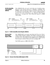
...MSR C000_0087h. 9 87 432 0 N O L STEP BF 2 Reserved Symbol Description Bit NOL2 No L2 Functionality 8 STEP Processor Stepping 7-4 BF Bus Frequency Divisor 2-0 Figure 38. The PSOR is defined as uncacheable (UC) or write-combining (WC) memory. For a description ... 10 Physical Base Address 1 WU Physical Address Mask 1 C C 11 Physical Base Address 0 WU Physical Address Mask 0 C C 00 MTRR1 MTRR0 Figure 37. UC/WC Cacheability Control Register (UWCCR) Processor State Observability Register (PSOR) . 63 The AMD-K6-2E+ processor provides the Processor State Observability...
...MSR C000_0087h. 9 87 432 0 N O L STEP BF 2 Reserved Symbol Description Bit NOL2 No L2 Functionality 8 STEP Processor Stepping 7-4 BF Bus Frequency Divisor 2-0 Figure 38. The PSOR is defined as uncacheable (UC) or write-combining (WC) memory. For a description ... 10 Physical Base Address 1 WU Physical Address Mask 1 C C 11 Physical Base Address 0 WU Physical Address Mask 0 C C 00 MTRR1 MTRR0 Figure 37. UC/WC Cacheability Control Register (UWCCR) Processor State Observability Register (PSOR) . 63 The AMD-K6-2E+ processor provides the Processor State Observability...
User Guide
Page 173
... must be prevented during the EPM Stop Grant state. s Based on its VID[4:0] inputs, the regulator outputs a corresponding voltage. Chapter 6 AMD PowerNow!™ Technology 151 23542A/0-September 2000 Preliminary Information AMD-K6™-2E+ Embedded Processor Data Sheet Dynamic Core Frequency Control Voltage Identification (VID) Outputs For AMD PowerNow! s These outputs serve as inputs to a DC/DC...
... must be prevented during the EPM Stop Grant state. s Based on its VID[4:0] inputs, the regulator outputs a corresponding voltage. Chapter 6 AMD PowerNow!™ Technology 151 23542A/0-September 2000 Preliminary Information AMD-K6™-2E+ Embedded Processor Data Sheet Dynamic Core Frequency Control Voltage Identification (VID) Outputs For AMD PowerNow! s These outputs serve as inputs to a DC/DC...