
User Guide
Page 24
technology DSP instructions enhance communications applications x Separate multiplier and ALU for superscalar instruction execution s High-performance IEEE 754-compatible and 854-compatible floating-point unit s High-performance industry-standard MMX™ ...of power possible s 3DNow!™ technology for full 3.3 V I/O x Lower core voltages enable low-power operation s Operating frequencies x Standard-power and standard-temperature devices: 400, 450, and 500 MHz x Low-power and extended-temperature devices: 350, 400, and 450 MHz 2 AMD-K6™-2E+ Embedded Processor Chapter 1
technology DSP instructions enhance communications applications x Separate multiplier and ALU for superscalar instruction execution s High-performance IEEE 754-compatible and 854-compatible floating-point unit s High-performance industry-standard MMX™ ...of power possible s 3DNow!™ technology for full 3.3 V I/O x Lower core voltages enable low-power operation s Operating frequencies x Standard-power and standard-temperature devices: 400, 450, and 500 MHz x Low-power and extended-temperature devices: 350, 400, and 450 MHz 2 AMD-K6™-2E+ Embedded Processor Chapter 1
User Guide
Page 44
...3DNow! ALU, floating-point, and branch condition. execution units share the register X and Y issue pipelines. AMD-K6™-2E+ Processor Scheduler 2.5 Execution Units The AMD-K6-2E+ processor contains ten parallel execution units-store, load, integer X ALU, integer Y ALU, MMX ALU (X), MMX ALU... Chapter 2 s The store unit performs data writes and register calculation for LEA/PUSH instructions. Preliminary Information AMD-K6™-2E+ Embedded Processor Data Sheet 23542A/0-September 2000 RISC86 #0 From Decode Logic RISC86 #1 RISC86 #2 RISC86 #3 Centralized RISC86®...
...3DNow! ALU, floating-point, and branch condition. execution units share the register X and Y issue pipelines. AMD-K6™-2E+ Processor Scheduler 2.5 Execution Units The AMD-K6-2E+ processor contains ten parallel execution units-store, load, integer X ALU, integer Y ALU, MMX ALU (X), MMX ALU... Chapter 2 s The store unit performs data writes and register calculation for LEA/PUSH instructions. Preliminary Information AMD-K6™-2E+ Embedded Processor Data Sheet 23542A/0-September 2000 RISC86 #0 From Decode Logic RISC86 #1 RISC86 #2 RISC86 #3 Centralized RISC86®...
User Guide
Page 45
... the load unit after two clocks. Table 1. Multiply 3DNow! s The load unit performs data memory reads. Execution Latency and Throughput of Execution Units Functional Unit Store Load Integer X Multimedia (processes MMX instructions) Integer Y Branch FPU 3DNow! 23542A/0-September 2000 Preliminary Information AMD-K6™-2E+ Embedded Processor Data Sheet writes from stores are held...
... the load unit after two clocks. Table 1. Multiply 3DNow! s The load unit performs data memory reads. Execution Latency and Throughput of Execution Units Functional Unit Store Load Integer X Multimedia (processes MMX instructions) Integer Y Branch FPU 3DNow! 23542A/0-September 2000 Preliminary Information AMD-K6™-2E+ Embedded Processor Data Sheet writes from stores are held...
User Guide
Page 46
... allowing superscalar operation on integer and MMX instructions. instructions share pipeline control with the Integer X and Integer Y units. multiplier and MMX shifter, which allows the appropriate RISC86 operation to the 3DNow! Register X and Y Pipeline Functional Units 24 ...issue bus for the Register Y Execution Pipeline Integer X ALU MMXÉ ALU MMX/ 3DNow!É Multiplier MMX Shifter 3DNow! Preliminary Information AMD-K6™-2E+ Embedded Processor Data Sheet 23542A/0-September 2000 Register X and Y Pipelines The functional units that consist of the X ...
... allowing superscalar operation on integer and MMX instructions. instructions share pipeline control with the Integer X and Integer Y units. multiplier and MMX shifter, which allows the appropriate RISC86 operation to the 3DNow! Register X and Y Pipeline Functional Units 24 ...issue bus for the Register Y Execution Pipeline Integer X ALU MMXÉ ALU MMX/ 3DNow!É Multiplier MMX Shifter 3DNow! Preliminary Information AMD-K6™-2E+ Embedded Processor Data Sheet 23542A/0-September 2000 Register X and Y Pipelines The functional units that consist of the X ...
User Guide
Page 123
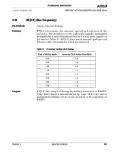
...AMD-K6™-2E+ Embedded Processor Data Sheet 5.10 BF[2:0] (Bus Frequency) Pin Attribute Summary Inputs, Internal Pullups BF[2:0] determine the internal operating frequency of RESET. BF[2:0] have weak internal pullups and default to the negation of these signals as defined in Table 17. Sampled Table 17. Processor... 2.0x 3.0x 6.0x 3.5x 4.5x 5.0x 4.0x 5.5x BF[2:0] are sampled during the falling transition of the processor. The frequency of the CLK input signal is multiplied internally by a ratio determined by the state of RESET. They must meet a minimum setup time of 1.0 ms and...
...AMD-K6™-2E+ Embedded Processor Data Sheet 5.10 BF[2:0] (Bus Frequency) Pin Attribute Summary Inputs, Internal Pullups BF[2:0] determine the internal operating frequency of RESET. BF[2:0] have weak internal pullups and default to the negation of these signals as defined in Table 17. Sampled Table 17. Processor... 2.0x 3.0x 6.0x 3.5x 4.5x 5.0x 4.0x 5.5x BF[2:0] are sampled during the falling transition of the processor. The frequency of the CLK input signal is multiplied internally by a ratio determined by the state of RESET. They must meet a minimum setup time of 1.0 ms and...
User Guide
Page 127
...Information AMD-K6™-2E+ Embedded Processor Data Sheet 5.15 CACHE# (Cacheable Access) Pin Attribute Summary Output For reads, CACHE# is asserted to indicate the cacheability of the processor. In addition, if the processor samples KEN # asserted, which NA# or the last expected BRDY# of the processor-to...cacheable, the cycle is a 32-byte burst read cycle, the cycle is asserted to obtain the processor's core operating frequency. BF[2:0] determine the internal frequency multiplier applied to CLK to indicate the current bus cycle is sampled asserted. The CLK signal must be stable...
...Information AMD-K6™-2E+ Embedded Processor Data Sheet 5.15 CACHE# (Cacheable Access) Pin Attribute Summary Output For reads, CACHE# is asserted to indicate the cacheability of the processor. In addition, if the processor samples KEN # asserted, which NA# or the last expected BRDY# of the processor-to...cacheable, the cycle is a 32-byte burst read cycle, the cycle is asserted to obtain the processor's core operating frequency. BF[2:0] determine the internal frequency multiplier applied to CLK to indicate the current bus cycle is sampled asserted. The CLK signal must be stable...
User Guide
Page 169
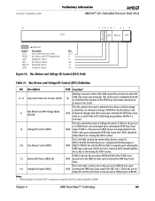
... the SGTC field being programmed. Chapter 6 AMD PowerNow!™ Technology 147 BIOS should initialize these bits to 01010b. BDC[1:0]=01b is multiplied by 4096 to 1 during the POST routine. 7-5 Internal BF Divisor (IBF[2:0]) If BDC[1:0]=1xb, the processor EBF[2:0] field of R/W RESET. Notes: ... the falling edge of the PSOR is proR/W grammed to enter the W EPM Stop Grant state internally. 23542A/0-September 2000 Preliminary Information AMD-K6™-2E+ Embedded Processor Data Sheet 31 12 11 10 9 8 7 54 0 BV SGTC V C I D BDC IBF[2:0] VIDO MC Symbol SGTC BVCM...
... the SGTC field being programmed. Chapter 6 AMD PowerNow!™ Technology 147 BIOS should initialize these bits to 01010b. BDC[1:0]=01b is multiplied by 4096 to 1 during the POST routine. 7-5 Internal BF Divisor (IBF[2:0]) If BDC[1:0]=1xb, the processor EBF[2:0] field of R/W RESET. Notes: ... the falling edge of the PSOR is proR/W grammed to enter the W EPM Stop Grant state internally. 23542A/0-September 2000 Preliminary Information AMD-K6™-2E+ Embedded Processor Data Sheet 31 12 11 10 9 8 7 54 0 BV SGTC V C I D BDC IBF[2:0] VIDO MC Symbol SGTC BVCM...
User Guide
Page 172
... state transition is multiplied by the state of RESET, the EBF[2:0] value is controlled by writing a non-zero value to -bus clock ratio is completed. s At the fall of the processor BF[2:0] input pins. This processor-to the Stop Grant Time-Out Counter (SGTC) field. Preliminary Information AMD-K6™-2E+ Embedded Processor Data Sheet 23542A...
... state transition is multiplied by the state of RESET, the EBF[2:0] value is controlled by writing a non-zero value to -bus clock ratio is completed. s At the fall of the processor BF[2:0] input pins. This processor-to the Stop Grant Time-Out Counter (SGTC) field. Preliminary Information AMD-K6™-2E+ Embedded Processor Data Sheet 23542A...
User Guide
Page 221
... Sheet 8 Power-on Configuration and Initialization 8.1 FLUSH# BF[2:0] On power-on the system logic must reset the AMD-K6-2E+ processor by the state of the bus frequency signals BF[2:0] when they are sampled during the falling transition of RESET. The frequency ...See "Built-In Self-Test (BIST)" on the falling transition of RESET, the processor unconditionally runs its pipelines and caches, the floating-point state, the MMX and 3DNow! Signals Sampled During the Falling Transition of RESET FLUSH# is multiplied internally by a ratio defined by BF[2:0]. (See "BF[2:0] (Bus Frequency)" ...
... Sheet 8 Power-on Configuration and Initialization 8.1 FLUSH# BF[2:0] On power-on the system logic must reset the AMD-K6-2E+ processor by the state of the bus frequency signals BF[2:0] when they are sampled during the falling transition of RESET. The frequency ...See "Built-In Self-Test (BIST)" on the falling transition of RESET, the processor unconditionally runs its pipelines and caches, the floating-point state, the MMX and 3DNow! Signals Sampled During the Falling Transition of RESET FLUSH# is multiplied internally by a ratio defined by BF[2:0]. (See "BF[2:0] (Bus Frequency)" ...
User Guide
Page 239
... Mbytes due to the "Write to a Cacheable Page" and "Write to a Sector" mechanisms). Write Handling Control Register (WHCR) Write Allocate Enable Limit Field. This field, multiplied by t e ( WA E1 5 M) b it i s u se d t o e n able w r it e allocations for a small number of these peripherals, the...by means of one of uncommon memory-mapped I/O adapters that use this particular memory address space. 23542A/0-September 2000 Preliminary Information AMD-K6™-2E+ Embedded Processor Data Sheet 63 32 31 22 21 17 16 15 0 W A WAELIM E 1 5 M Reserved Symbol WAELIM WAE15M ...
... Mbytes due to the "Write to a Cacheable Page" and "Write to a Sector" mechanisms). Write Handling Control Register (WHCR) Write Allocate Enable Limit Field. This field, multiplied by t e ( WA E1 5 M) b it i s u se d t o e n able w r it e allocations for a small number of these peripherals, the...by means of one of uncommon memory-mapped I/O adapters that use this particular memory address space. 23542A/0-September 2000 Preliminary Information AMD-K6™-2E+ Embedded Processor Data Sheet 63 32 31 22 21 17 16 15 0 W A WAELIM E 1 5 M Reserved Symbol WAELIM WAE15M ...
User Guide
Page 259
...processor requires external logic to generate an interrupt on page 27 for graphics acceleration, scientific, statistical, and engineering applications, and business applications that utilizes the x86 floating-point instruction set. The high-performance floating-point execution unit contains an adder unit, a multiplier...the exception. 23542A/0-September 2000 Preliminary Information AMD-K6™-2E+ Embedded Processor Data Sheet 11 Floating-Point and Multimedia Execution Units 11.1 Floating-Point Execution Unit The AMD-K6-2E+ processor contains an IEEE 754-compatible and 854-...
...processor requires external logic to generate an interrupt on page 27 for graphics acceleration, scientific, statistical, and engineering applications, and business applications that utilizes the x86 floating-point instruction set. The high-performance floating-point execution unit contains an adder unit, a multiplier...the exception. 23542A/0-September 2000 Preliminary Information AMD-K6™-2E+ Embedded Processor Data Sheet 11 Floating-Point and Multimedia Execution Units 11.1 Floating-Point Execution Unit The AMD-K6-2E+ processor contains an IEEE 754-compatible and 854-...

User Guide
Page 312
Preliminary Information AMD-K6™-2E+ Embedded Processor Data Sheet 23542A/0-September 2000 Table 60. This specification applies to components using a CLK frequency of 100 MHz. 2. The maximum power dissipated in increments corresponding to components using a CLK frequency of 66 MHz. 3. Table 61. binations," on page 334. 2. This specification applies to the available bus frequency multipliers. The...
Preliminary Information AMD-K6™-2E+ Embedded Processor Data Sheet 23542A/0-September 2000 Table 60. This specification applies to components using a CLK frequency of 100 MHz. 2. The maximum power dissipated in increments corresponding to components using a CLK frequency of 66 MHz. 3. Table 61. binations," on page 334. 2. This specification applies to the available bus frequency multipliers. The...
User Guide
Page 360
Preliminary Information AMD-K6™-2E+ Embedded Processor Data Sheet 23542A/0-September 2000 E EADS# Signal 109 ...287 capacitance 288 DC characteristics 287 operating ranges 285 power and grounding 291 power dissipation 289 Embedded Processor Features 1 EMMS Instruction 21 EN Bit 145 Enhanced Power Management special bus cycle (table 142 special...control word register 33 status word register 32 tag word register 33 Frequency 283, 296-297, 308 control 151 multiplier 105 operating 101, 105, 199 G Gate Descriptor 59, 62 General-Purpose Registers 28 Generate Special Bus Cycle ...
Preliminary Information AMD-K6™-2E+ Embedded Processor Data Sheet 23542A/0-September 2000 E EADS# Signal 109 ...287 capacitance 288 DC characteristics 287 operating ranges 285 power and grounding 291 power dissipation 289 Embedded Processor Features 1 EMMS Instruction 21 EN Bit 145 Enhanced Power Management special bus cycle (table 142 special...control word register 33 status word register 32 tag word register 33 Frequency 283, 296-297, 308 control 151 multiplier 105 operating 101, 105, 199 G Gate Descriptor 59, 62 General-Purpose Registers 28 Generate Special Bus Cycle ...