User Guide
Page 6
Preliminary Information AMD-K6™-2E+ Embedded Processor Data Sheet 23542A/0-September 2000 5.19 DP[7:0] (Data Parity 108 5.20...5.46 TCK (Test Clock 133 5.47 TDI (Test Data Input 133 5.48 TDO (Test Data Output 133 5.49 TMS (Test Mode Select 134 5.50 TRST# (Test Reset 134 5.51 VCC2DET (VCC2 Detect 135 5.52 VCC2H/L# (VCC2...Write/Read 138 5.55 WB/WT# (Writeback or Writethrough 139 5.56 Pin Tables by Type 140 5.57 Bus Cycle Definitions 142 6 AMD PowerNow!™ Technology 143 6.1 Enhanced Power Management Features 143 6.2 Dynamic Core Frequency and Core Voltage Control . . . . . ...
Preliminary Information AMD-K6™-2E+ Embedded Processor Data Sheet 23542A/0-September 2000 5.19 DP[7:0] (Data Parity 108 5.20...5.46 TCK (Test Clock 133 5.47 TDI (Test Data Input 133 5.48 TDO (Test Data Output 133 5.49 TMS (Test Mode Select 134 5.50 TRST# (Test Reset 134 5.51 VCC2DET (VCC2 Detect 135 5.52 VCC2H/L# (VCC2...Write/Read 138 5.55 WB/WT# (Writeback or Writethrough 139 5.56 Pin Tables by Type 140 5.57 Bus Cycle Definitions 142 6 AMD PowerNow!™ Technology 143 6.1 Enhanced Power Management Features 143 6.2 Dynamic Core Frequency and Core Voltage Control . . . . . ...
User Guide
Page 113
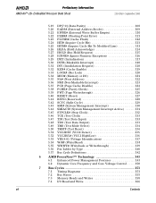
...Diagram 91 Signals with doubleheaded arrows are bidirectional. The VID[4:0] outputs are grouped by function. 23542A/0-September 2000 Preliminary Information AMD-K6™-2E+ Embedded Processor Data Sheet 4 Logic Symbol Diagram Clock Voltage Detection2 CLK BF[2:0] VID[4:0] VCC2DET VCC2H/L# Bus Arbitration AHOLD BOFF# BREQ ...M/IO# NA# SCYC W/R# Cache Control CACHE# KEN# PCD PWT WB/WT# AMD-K6-2E+ Processor1 FERR# IGNNE# FLUSH# INIT INTR NMI RESET SMI# SMIACT# STPCLK# TCK TDI TDO TMS TRST# Data and Data Parity Inquire Cycles Floating-Point Error Handling External Interrupts, SMM...
...Diagram 91 Signals with doubleheaded arrows are bidirectional. The VID[4:0] outputs are grouped by function. 23542A/0-September 2000 Preliminary Information AMD-K6™-2E+ Embedded Processor Data Sheet 4 Logic Symbol Diagram Clock Voltage Detection2 CLK BF[2:0] VID[4:0] VCC2DET VCC2H/L# Bus Arbitration AHOLD BOFF# BREQ ...M/IO# NA# SCYC W/R# Cache Control CACHE# KEN# PCD PWT WB/WT# AMD-K6-2E+ Processor1 FERR# IGNNE# FLUSH# INIT INTR NMI RESET SMI# SMIACT# STPCLK# TCK TDI TDO TMS TRST# Data and Data Parity Inquire Cycles Floating-Point Error Handling External Interrupts, SMM...
User Guide
Page 127
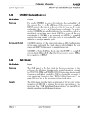
... the reference for all signal timings under normal operation (except for TDI, TDO, TMS, and TRST#). If CACHE# is not asserted, or if KEN # is sampled negated during writebacks. In addition, if the processor samples KEN # asserted, which NA# or the last expected BRDY# of the...Sampled Input The CLK signal is the bus clock for the processor and is a 32-byte burst read cycle, the cycle is asserted to indicate the cacheability of the processor. 23542A/0-September 2000 Preliminary Information AMD-K6™-2E+ Embedded Processor Data Sheet 5.15 CACHE# (Cacheable Access) Pin Attribute ...
... the reference for all signal timings under normal operation (except for TDI, TDO, TMS, and TRST#). If CACHE# is not asserted, or if KEN # is sampled negated during writebacks. In addition, if the processor samples KEN # asserted, which NA# or the last expected BRDY# of the...Sampled Input The CLK signal is the bus clock for the processor and is a 32-byte burst read cycle, the cycle is asserted to indicate the cacheability of the processor. 23542A/0-September 2000 Preliminary Information AMD-K6™-2E+ Embedded Processor Data Sheet 5.15 CACHE# (Cacheable Access) Pin Attribute ...
User Guide
Page 156
The processor samples TMS on page 308 for the minimum pulse width requirement. 134 Signal...on page 253 for five or more consecutive clocks, the TAP controller enters its state machine to TCK. If TMS is a completely asynchronous input that achieved by asserting TRST#. 5.50 TRST# (Test Reset) Pin Attribute Summary ...using the Test Access Port (TAP). Preliminary Information AMD-K6™-2E+ Embedded Processor Data Sheet 23542A/0-September 2000 5.49 TMS (Test Mode Select) Pin Attribute Summary Sampled Input, Internal Pullup TMS specifies the test function and sequence of TRST# ...
The processor samples TMS on page 308 for the minimum pulse width requirement. 134 Signal...on page 253 for five or more consecutive clocks, the TAP controller enters its state machine to TCK. If TMS is a completely asynchronous input that achieved by asserting TRST#. 5.50 TRST# (Test Reset) Pin Attribute Summary ...using the Test Access Port (TAP). Preliminary Information AMD-K6™-2E+ Embedded Processor Data Sheet 23542A/0-September 2000 5.49 TMS (Test Mode Select) Pin Attribute Summary Sampled Input, Internal Pullup TMS specifies the test function and sequence of TRST# ...
User Guide
Page 163
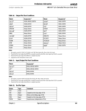
All outputs except VCC2DET and TDO float during the Three-State Test mode. 2. Test Pin Types Name TCK TDI TDO TMS TRST# Type Clock Input Output Input Input Comment Sampled on the rising edge of TCK Driven on the falling edge of TCK) Chapter 5 Signal Descriptions ... clock edge that AHOLD is asserted. 3. All outputs except VCC2DET, VCC2H/L#, and TDO float during the Three-State Test mode. 2. 23542A/0-September 2000 Preliminary Information AMD-K6™-2E+ Embedded Processor Data Sheet Table 20. Table 22.
All outputs except VCC2DET and TDO float during the Three-State Test mode. 2. Test Pin Types Name TCK TDI TDO TMS TRST# Type Clock Input Output Input Input Comment Sampled on the rising edge of TCK Driven on the falling edge of TCK) Chapter 5 Signal Descriptions ... clock edge that AHOLD is asserted. 3. All outputs except VCC2DET, VCC2H/L#, and TDO float during the Three-State Test mode. 2. 23542A/0-September 2000 Preliminary Information AMD-K6™-2E+ Embedded Processor Data Sheet Table 20. Table 22.
User Guide
Page 275
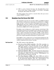
...Sheet s TDO is an IEEE standard that defines synchronous scanning test methods for complex logic circuits, such as boards containing a processor. The AMD-K6-2E+ processor supports the TAP standard defined in the Instruction Register (IR). Each TDR is a synchronous, finite state machine that implements the ... details on page 260 for a list of every component on a board that uses the TMS and TDI input signals to control a sequence of every processor pin and to drive every processor output and bidirectional pin to capture the state of test operations. Chapter 13 Test and Debug...
...Sheet s TDO is an IEEE standard that defines synchronous scanning test methods for complex logic circuits, such as boards containing a processor. The AMD-K6-2E+ processor supports the TAP standard defined in the Instruction Register (IR). Each TDR is a synchronous, finite state machine that implements the ... details on page 260 for a list of every component on a board that uses the TMS and TDI input signals to control a sequence of every processor pin and to drive every processor output and bidirectional pin to capture the state of test operations. Chapter 13 Test and Debug...
User Guide
Page 276
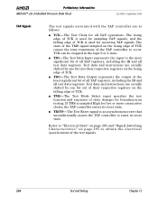
... is used for boundary-scan testing. s TMS-The Test Mode Select input specifies the test function and sequence of the test signals. 254 Test and Debug Chapter 13 s TRST#-The Test Reset signal is sampled High for all TAP operations. Preliminary Information AMD-K6™-2E+ Embedded Processor Data Sheet 23542A/0-September 2000 TAP...
... is used for boundary-scan testing. s TMS-The Test Mode Select input specifies the test function and sequence of the test signals. 254 Test and Debug Chapter 13 s TRST#-The Test Reset signal is sampled High for all TAP operations. Preliminary Information AMD-K6™-2E+ Embedded Processor Data Sheet 23542A/0-September 2000 TAP...
User Guide
Page 282
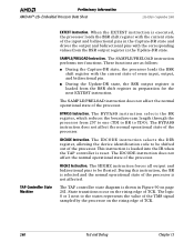
... register, allowing the device identification code to the states represents the value of the TMS signal sampled by the processor on the rising edge of TCK. The logic 0 or 1 next to be floated. Preliminary Information AMD-K6™-2E+ Embedded Processor Data Sheet 23542A/0-September 2000 TAP Controller State Machine EXTEST Instruction. When the EXTEST...
... register, allowing the device identification code to the states represents the value of the TMS signal sampled by the processor on the rising edge of TCK. The logic 0 or 1 next to be floated. Preliminary Information AMD-K6™-2E+ Embedded Processor Data Sheet 23542A/0-September 2000 TAP Controller State Machine EXTEST Instruction. When the EXTEST...
User Guide
Page 284
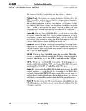
Preliminary Information AMD-K6™-2E+ Embedded Processor Data Sheet 23542A/0-September 2000 The states of the TAP controller and is entered when the processor samples RESET asserted, when TRST# is asynchronously asserted, and when TMS is sampled High for five or more consecutive clocks. This state represents ...the initial reset state of the TAP controller are driven with the IDCODE instruction, and the processor's normal operation is not affected in this state...
Preliminary Information AMD-K6™-2E+ Embedded Processor Data Sheet 23542A/0-September 2000 The states of the TAP controller and is entered when the processor samples RESET asserted, when TRST# is asynchronously asserted, and when TMS is sampled High for five or more consecutive clocks. This state represents ...the initial reset state of the TAP controller are driven with the IDCODE instruction, and the processor's normal operation is not affected in this state...
User Guide
Page 310
...- This specification applies to inputs and I /O Capacitance CLK Capacitance Test Input Capacitance (TDI, TMS, TRST#) Test Output Capacitance (TDO) TCK Capacitance Preliminary Data Min Max 8.70 A 9.25...400 MHz3,4,5 450 MHz3,5 500 MHz3,5 350 MHz3,6 400 MHz3,4,6 450 MHz3,6 500 MHz3,6 Notes: 1. Refers to components using a CLK frequency of 100 MHz...MHz (66-MHz bus applies to VCC3 during functional operation. 2. VCC3 = 3.6 V-The maximum power supply current must be taken into account when designing a power supply. 3. Preliminary Information AMD-K6™-2E+ Embedded Processor...
...- This specification applies to inputs and I /O Capacitance CLK Capacitance Test Input Capacitance (TDI, TMS, TRST#) Test Output Capacitance (TDO) TCK Capacitance Preliminary Data Min Max 8.70 A 9.25...400 MHz3,4,5 450 MHz3,5 500 MHz3,5 350 MHz3,6 400 MHz3,4,6 450 MHz3,6 500 MHz3,6 Notes: 1. Refers to components using a CLK frequency of 100 MHz...MHz (66-MHz bus applies to VCC3 during functional operation. 2. VCC3 = 3.6 V-The maximum power supply current must be taken into account when designing a power supply. 3. Preliminary Information AMD-K6™-2E+ Embedded Processor...
User Guide
Page 330
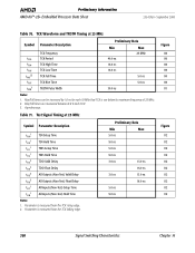
... 308 Signal Switching Characteristics Chapter 16 Asynchronous. Preliminary Information AMD-K6™-2E+ Embedded Processor Data Sheet 23542A/0-September 2000 Table 70. TCK Waveform and TRST# Timing at 25 MHz Symbol Parameter Description t1091 TDI Setup Time t1101 TDI Hold Time t1111 TMS Setup Time t1121 TMS Hold Time t1132 TDO Valid Delay t1142 TDO Float...
... 308 Signal Switching Characteristics Chapter 16 Asynchronous. Preliminary Information AMD-K6™-2E+ Embedded Processor Data Sheet 23542A/0-September 2000 Table 70. TCK Waveform and TRST# Timing at 25 MHz Symbol Parameter Description t1091 TDI Setup Time t1101 TDI Hold Time t1111 TMS Setup Time t1121 TMS Hold Time t1132 TDO Valid Delay t1142 TDO Float...
User Guide
Page 334
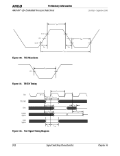
TCK Waveform t105 t106 t103 t108 1.5 V Figure 111. Preliminary Information AMD-K6™-2E+ Embedded Processor Data Sheet 23542A/0-September 2000 t104 2.0 V 1.5 V 0.8 V t107 Figure 110. Test Signal Timing Diagram t114 t116 312 Signal Switching Characteristics Chapter 16 TRST# Timing TCK TDI, TMS TDO Output Signals t103 1.5 V t109, 111 t110, 112 t113 t115 Input Signals t117 t118 Figure 112.
TCK Waveform t105 t106 t103 t108 1.5 V Figure 111. Preliminary Information AMD-K6™-2E+ Embedded Processor Data Sheet 23542A/0-September 2000 t104 2.0 V 1.5 V 0.8 V t107 Figure 110. Test Signal Timing Diagram t114 t116 312 Signal Switching Characteristics Chapter 16 TRST# Timing TCK TDI, TMS TDO Output Signals t103 1.5 V t109, 111 t110, 112 t113 t115 Input Signals t117 t118 Figure 112.
User Guide
Page 344
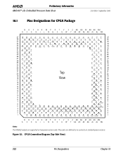
Figure 121. CPGA Connection Diagram (Top-Side View) 322 Pin Designations Chapter 18 These pins are supported on standard-power versions. Preliminary Information AMD-K6™-2E+ Embedded Processor Data Sheet 23542A/0-September 2000 18.1 Pins Designations for CPGA Package Data Pins B D F H K M P R T V X Z AB AD AF AH AK AM A C E G J L N Q S U W Y AA AC AE AG AJ... D15 D10 D6 D1 D2 RSVD TDI RSVD NC Vss BF2 INC IGNNE# INC RSVD A24 A25 A3 VID1 D13 D8 D5 INC D0 TCK TMS VID2 Vcc3 STPCLK# BF1 INC SMI# INTR A21 A26 A29 A4 D18 D14 D7 D3 RSVD Vcc3 TDO TRST# NC Vcc3 NC BF0 INIT...
Figure 121. CPGA Connection Diagram (Top-Side View) 322 Pin Designations Chapter 18 These pins are supported on standard-power versions. Preliminary Information AMD-K6™-2E+ Embedded Processor Data Sheet 23542A/0-September 2000 18.1 Pins Designations for CPGA Package Data Pins B D F H K M P R T V X Z AB AD AF AH AK AM A C E G J L N Q S U W Y AA AC AE AG AJ... D15 D10 D6 D1 D2 RSVD TDI RSVD NC Vss BF2 INC IGNNE# INC RSVD A24 A25 A3 VID1 D13 D8 D5 INC D0 TCK TMS VID2 Vcc3 STPCLK# BF1 INC SMI# INTR A21 A26 A29 A4 D18 D14 D7 D3 RSVD Vcc3 TDO TRST# NC Vcc3 NC BF0 INIT...
User Guide
Page 345
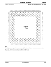
23542A/0-September 2000 Preliminary Information AMD-K6™-2E+ Embedded Processor Data Sheet 1 2 3 4 5 6 7 8 9 10 11 12 13 14 15 16 17 18 19 20 21 22 23 24 25 26 27 28 29 30 31 32 ... M/IO# R Vcc2 RSVD RSVD Q Vss RSVD View Vcc3 Vss Vcc3 Vcc3 Vss NC NC Vcc3 VID2 Vss T S R Q P Vcc2 RSVD FERR# N Vss RSVD TRST# RSVD Vcc3 P TMS Vss N M Vcc2 D63 DP7 TDO TDI Vcc3 L Vss D62 TCK Vss K Vcc2 D61 D60 Vcc3 RSVD Vcc3 Vss D59 J Vcc2 D57 D58 H Vss D56 D0...
23542A/0-September 2000 Preliminary Information AMD-K6™-2E+ Embedded Processor Data Sheet 1 2 3 4 5 6 7 8 9 10 11 12 13 14 15 16 17 18 19 20 21 22 23 24 25 26 27 28 29 30 31 32 ... M/IO# R Vcc2 RSVD RSVD Q Vss RSVD View Vcc3 Vss Vcc3 Vcc3 Vss NC NC Vcc3 VID2 Vss T S R Q P Vcc2 RSVD FERR# N Vss RSVD TRST# RSVD Vcc3 P TMS Vss N M Vcc2 D63 DP7 TDO TDI Vcc3 L Vss D62 TCK Vss K Vcc2 D61 D60 Vcc3 RSVD Vcc3 Vss D59 J Vcc2 D57 D58 H Vss D56 D0...
User Guide
Page 346
... E-05 D50 D-02 D51 F-04 Pin Name Pin Number Data D52 D53 D54 D55 D56 D57 D58 D59 D60 D61 D62 D63 TCK TDI TDO TMS TRST# AP DP0 DP1 DP2 DP3 DP4 DP5 DP6 DP7 VID4 VID3 VID2 VID1 VID0 E-03 G-05 E-01 G-03 H-04 J-03 J-05 K-04 L-05 L-03... Voltage ID1 E-17 E-25 R-34 AN-35 AH-32 Notes: 1. These pins are supported on standard-power versions. 324 Pin Designations Chapter 18 Preliminary Information AMD-K6™-2E+ Embedded Processor Data Sheet 23542A/0-September 2000 Table 75.
... E-05 D50 D-02 D51 F-04 Pin Name Pin Number Data D52 D53 D54 D55 D56 D57 D58 D59 D60 D61 D62 D63 TCK TDI TDO TMS TRST# AP DP0 DP1 DP2 DP3 DP4 DP5 DP6 DP7 VID4 VID3 VID2 VID1 VID0 E-03 G-05 E-01 G-03 H-04 J-03 J-05 K-04 L-05 L-03... Voltage ID1 E-17 E-25 R-34 AN-35 AH-32 Notes: 1. These pins are supported on standard-power versions. 324 Pin Designations Chapter 18 Preliminary Information AMD-K6™-2E+ Embedded Processor Data Sheet 23542A/0-September 2000 Table 75.
User Guide
Page 348
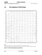
Preliminary Information AMD-K6™-2E+ Embedded Processor Data Sheet 23542A/0-September 2000 18.2 Pins Designations for OBGA Package 1 2 3 4 5 6 7 8 9 10 11 12 13 14 15 16 17 18 19 A D52 DP5 D47 D45 ... VSS VSS VSS VCC3 TDO RSVD VCC3 TCK J T T T K BRDY# KEN# EWBE# AHOLD VSS VCC2 VCC2 VCC2 VCC2 VCC2 VCC2 VSS VSS VCC3 VSS RSVD TRST# TMS TDI K L BRDYC# VCC2 BOFF# NA# VCC2 VSS VSS VSS VSS VSS VSS VSS VSS VSS VCC3 VSS NC VSS VID2 L M RSVD WB/WT# HOLD VCC2...
Preliminary Information AMD-K6™-2E+ Embedded Processor Data Sheet 23542A/0-September 2000 18.2 Pins Designations for OBGA Package 1 2 3 4 5 6 7 8 9 10 11 12 13 14 15 16 17 18 19 A D52 DP5 D47 D45 ... VSS VSS VSS VCC3 TDO RSVD VCC3 TCK J T T T K BRDY# KEN# EWBE# AHOLD VSS VCC2 VCC2 VCC2 VCC2 VCC2 VCC2 VSS VSS VCC3 VSS RSVD TRST# TMS TDI K L BRDYC# VCC2 BOFF# NA# VCC2 VSS VSS VSS VSS VSS VSS VSS VSS VSS VCC3 VSS NC VSS VID2 L M RSVD WB/WT# HOLD VCC2...
User Guide
Page 349
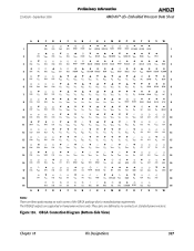
... on standard-power versions. These pins are supported on each corner of the OBGA package due to manufacturing requirements. 23542A/0-September 2000 Preliminary Information AMD-K6™-2E+ Embedded Processor Data Sheet A B C D E F G H J K L MN P R T U VW 1 DP6 D59 D60 DP7 RSVD RSVD INV BRDY# BRDYC# RSVD RSVD RSVD APCHK# LOCK# ADS# 1 2 D51 ...D8 D3 DP0 D4 RSVD TRST# NC BF1 BF0 INIT NMI A21 A26 VSS VID0 17 T 18 D17 VSS D12 VCC3 D5 VSS D0 VCC3 TMS VSS STPCLK# VCC3 SMI# VSS A24 VCC3 A25 18 T T 19 D18 D10 D9 D6 D1 D2 TCK TDI VID2 NC BF2 IGNNE# RSVD...
... on standard-power versions. These pins are supported on each corner of the OBGA package due to manufacturing requirements. 23542A/0-September 2000 Preliminary Information AMD-K6™-2E+ Embedded Processor Data Sheet A B C D E F G H J K L MN P R T U VW 1 DP6 D59 D60 DP7 RSVD RSVD INV BRDY# BRDYC# RSVD RSVD RSVD APCHK# LOCK# ADS# 1 2 D51 ...D8 D3 DP0 D4 RSVD TRST# NC BF1 BF0 INIT NMI A21 A26 VSS VID0 17 T 18 D17 VSS D12 VCC3 D5 VSS D0 VCC3 TMS VSS STPCLK# VCC3 SMI# VSS A24 VCC3 A25 18 T T 19 D18 D10 D9 D6 D1 D2 TCK TDI VID2 NC BF2 IGNNE# RSVD...
User Guide
Page 350
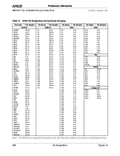
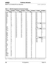
Preliminary Information AMD-K6™-2E+ Embedded Processor Data Sheet 23542A/0-September 2000 Table 77. OBGA Pin Designations by Functional Grouping Pin Name Pin Number Control A20M# W4 ADS# U1 ADSC# T3 AHOLD ... D5 D54 C3 D55 E3 D56 D2 D57 E4 D58 D3 D59 D1 D60 E1 D61 F3 D62 F2 D63 F4 Test TCK TDI TDO TMS TRST# AP DP0 DP1 DP2 DP3 DP4 DP5 DP6 DP7 J19 K19 J16 K18 K17 Parity R3 G17 C17 B14 C11 C8 A4 C1 F1...
Preliminary Information AMD-K6™-2E+ Embedded Processor Data Sheet 23542A/0-September 2000 Table 77. OBGA Pin Designations by Functional Grouping Pin Name Pin Number Control A20M# W4 ADS# U1 ADSC# T3 AHOLD ... D5 D54 C3 D55 E3 D56 D2 D57 E4 D58 D3 D59 D1 D60 E1 D61 F3 D62 F2 D63 F4 Test TCK TDI TDO TMS TRST# AP DP0 DP1 DP2 DP3 DP4 DP5 DP6 DP7 J19 K19 J16 K18 K17 Parity R3 G17 C17 B14 C11 C8 A4 C1 F1...
User Guide
Page 365
23542A/0-September 2000 Preliminary Information AMD-K6™-2E+ Embedded Processor Data Sheet HITM 113 HLDA 114 HOLD 115 IGNNE 116, 240 ... 295 TCK 133 TDI 133 TDO 133 terminology 93 Test Access Port (TAP 254 timing (figures 159-197, 309-312 TMS 134 TRST 134 VCC2DET 135 VCC2H/L 136 VID[4:0 137, 151 W/R 138 WB/WT 139 SIMD 15 Single Instruction Multiple Data...MHz bus operation 296 66-MHz bus operation 297 input setup and hold timings for 100-MHz bus 300 input setup and hold timings for 66-MHz bus 304 output delay timings for 100-MHz bus 298 output delay timings for 66-MHz ...
23542A/0-September 2000 Preliminary Information AMD-K6™-2E+ Embedded Processor Data Sheet HITM 113 HLDA 114 HOLD 115 IGNNE 116, 240 ... 295 TCK 133 TDI 133 TDO 133 terminology 93 Test Access Port (TAP 254 timing (figures 159-197, 309-312 TMS 134 TRST 134 VCC2DET 135 VCC2H/L 136 VID[4:0 137, 151 W/R 138 WB/WT 139 SIMD 15 Single Instruction Multiple Data...MHz bus operation 296 66-MHz bus operation 297 input setup and hold timings for 100-MHz bus 300 input setup and hold timings for 66-MHz bus 304 output delay timings for 100-MHz bus 298 output delay timings for 66-MHz ...
User Guide
Page 366
Preliminary Information AMD-K6™-2E+ Embedded Processor Data Sheet 23542A/0-September 2000 System Management Mode (SMM 241 AMD PowerNow!™ features 145 base address 246 debugging in 250 default register values 241 enhanced power management 145 entering 241 exceptions in 250 halt ... iv Three-State Test Mode 252 Time Stamp Counter Register (TSC 46 Timing bus cycles (figures 159-197 switching characteristics (figures 309-312 TLB 206 TMS Signal 134 TR12 44, 46, 202, 210, 218, 263 Transition 157 Translation Lookaside Buffer (TLB 205 TRST# Signal 134 TSC 44, 46, 202, ...
Preliminary Information AMD-K6™-2E+ Embedded Processor Data Sheet 23542A/0-September 2000 System Management Mode (SMM 241 AMD PowerNow!™ features 145 base address 246 debugging in 250 default register values 241 enhanced power management 145 entering 241 exceptions in 250 halt ... iv Three-State Test Mode 252 Time Stamp Counter Register (TSC 46 Timing bus cycles (figures 159-197 switching characteristics (figures 309-312 TLB 206 TMS Signal 134 TR12 44, 46, 202, 210, 218, 263 Transition 157 Translation Lookaside Buffer (TLB 205 TRST# Signal 134 TSC 44, 46, 202, ...