Service Manual
Page 29
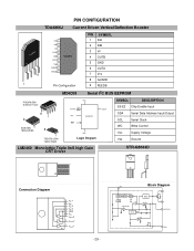
...) 0.25mm Frame SYMBOL DESCRIPTION E0-E2 Chip Enable Input 8 1 8 SO8 (MN) 1 150mil Width 8 1 TSSOP8 (DW) 169mil Width Logic Dirgram LM2469 Monolothic Triple 9nS high Gain CRT Driver SDA SCL WC Vcc Vss Serial Data Address Input/Output Serial Clock Write Control Supply Voltage Ground STR-G8644D Connection Diagram 9 1 9 VIN 1 8 7 6 5 4 3 VBB VIN 2 VIN...
...) 0.25mm Frame SYMBOL DESCRIPTION E0-E2 Chip Enable Input 8 1 8 SO8 (MN) 1 150mil Width 8 1 TSSOP8 (DW) 169mil Width Logic Dirgram LM2469 Monolothic Triple 9nS high Gain CRT Driver SDA SCL WC Vcc Vss Serial Data Address Input/Output Serial Clock Write Control Supply Voltage Ground STR-G8644D Connection Diagram 9 1 9 VIN 1 8 7 6 5 4 3 VBB VIN 2 VIN...
Service Manual
Page 30
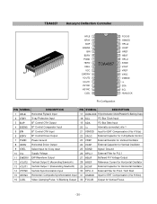
... EHT Compensation (Via V-Size) External Capacitor for V-Amplitude Control 7 PGND Power Ground 23 VREF External Resistor for Vertical Oscillator 8 HDRV Horizontal Driver Output 24 VCAP External Capacitor for Vertical Oscillator 9 XSEL Select Input for X-ray reset 25 SGND Signal Ground 10 Vcc Supply Voltage 26 HPLL1.../V-Blanking Output 2 XRAY 3 BOP 4 BSENS 5 BIN 6 BDRV X-ray Protection Input B+ Control OTA Output B+ Control Comparator Input B+ Control OTA Input B+ Control Driver Output 18 SCL 19 SDA 20 i.c 21 VSMOD 22 VAGC I2C-Bus Clock Input I2C-Bus Data Input Internally connected;
... EHT Compensation (Via V-Size) External Capacitor for V-Amplitude Control 7 PGND Power Ground 23 VREF External Resistor for Vertical Oscillator 8 HDRV Horizontal Driver Output 24 VCAP External Capacitor for Vertical Oscillator 9 XSEL Select Input for X-ray reset 25 SGND Signal Ground 10 Vcc Supply Voltage 26 HPLL1.../V-Blanking Output 2 XRAY 3 BOP 4 BSENS 5 BIN 6 BDRV X-ray Protection Input B+ Control OTA Output B+ Control Comparator Input B+ Control OTA Input B+ Control Driver Output 18 SCL 19 SDA 20 i.c 21 VSMOD 22 VAGC I2C-Bus Clock Input I2C-Bus Data Input Internally connected;
Service Guide
Page 13
... 14 through T402 (FBT) pin 7,C429, R449 and detected voltage feeding into negative pulse and sent to float HUNLOCK (pin17), H. HP S7500/MV7500/CV7500 3-3-1 Horizontal Section 1. The oscillatoris drivenby the currentsin R419 and R420. The minimumoscillator frequencyis determined by R419 and the maximum frequency is...(KA324) I402 and Q419 by R404, R406 and R405come into pin 2 of Vout2 can be activated to G1 for vertical blanking. 2. Horizontal driver (pin8) O/P to the vertical deflection booster pin 1 and pin 2 of TDA4841. The TDA4863 AJ has two output stages which are also...
... 14 through T402 (FBT) pin 7,C429, R449 and detected voltage feeding into negative pulse and sent to float HUNLOCK (pin17), H. HP S7500/MV7500/CV7500 3-3-1 Horizontal Section 1. The oscillatoris drivenby the currentsin R419 and R420. The minimumoscillator frequencyis determined by R419 and the maximum frequency is...(KA324) I402 and Q419 by R404, R406 and R405come into pin 2 of Vout2 can be activated to G1 for vertical blanking. 2. Horizontal driver (pin8) O/P to the vertical deflection booster pin 1 and pin 2 of TDA4841. The TDA4863 AJ has two output stages which are also...