
Data Sheet
Page 8
AMD-K6®-2 Processor Data Sheet ...249 13.2 Decoupling Recommendations 250 13.3 Pin Connection Requirements 251 14 Electrical Data 253 14.1 Electrical Data for OPN Suffixes AHX, 400AFQ, and AFR 253 Operating Ranges 253 ...Absolute Ratings 254 DC Characteristics 254 Power Dissipation 257 14.2 Electrical Data for OPN Suffixes AGR, AFX, and 400AFR 258 Operating Ranges 258 Absolute... 15 I/O Buffer Characteristics 263 15.1 Selectable Drive Strength 263 15.2 I/O Buffer Model 264 15.3 I/O Model Application Note 265 15.4 I/O Buffer AC and DC Characteristics 265 16 Signal Switching...
AMD-K6®-2 Processor Data Sheet ...249 13.2 Decoupling Recommendations 250 13.3 Pin Connection Requirements 251 14 Electrical Data 253 14.1 Electrical Data for OPN Suffixes AHX, 400AFQ, and AFR 253 Operating Ranges 253 ...Absolute Ratings 254 DC Characteristics 254 Power Dissipation 257 14.2 Electrical Data for OPN Suffixes AGR, AFX, and 400AFR 258 Operating Ranges 258 Absolute... 15 I/O Buffer Characteristics 263 15.1 Selectable Drive Strength 263 15.2 I/O Buffer Model 264 15.3 I/O Model Application Note 265 15.4 I/O Buffer AC and DC Characteristics 265 16 Signal Switching...

Data Sheet
Page 9
...2000 Preliminary Information AMD-K6®-2 Processor Data Sheet 16.5 Output Delay Timings for 100-MHz Bus Operation 270 16.6 Input Setup and Hold Timings for 100-MHz Bus Operation 272 16.7 Output Delay Timings for 66-MHz Bus Operation 274 16.8 Input Setup and Hold Timings for 66-MHz Bus Operation 276... 16.9 RESET and Test Signal Timing 278 17 Thermal Design 285 17.1 Package Thermal Specifications 285 Heat Dissipation Path 290 Measuring Case Temperature 290 17.2 Layout and ...
...2000 Preliminary Information AMD-K6®-2 Processor Data Sheet 16.5 Output Delay Timings for 100-MHz Bus Operation 270 16.6 Input Setup and Hold Timings for 100-MHz Bus Operation 272 16.7 Output Delay Timings for 66-MHz Bus Operation 274 16.8 Input Setup and Hold Timings for 66-MHz Bus Operation 276... 16.9 RESET and Test Signal Timing 278 17 Thermal Design 285 17.1 Package Thermal Specifications 285 Heat Dissipation Path 290 Measuring Case Temperature 290 17.2 Layout and ...

Data Sheet
Page 16
...Identifier 217 I/O Trap Dword Configuration 218 I/O Trap Restart Slot 219 Boundary Scan Bit Definitions for Model 8/[7:0 227 Boundary Scan Bit Definitions for Model 8/[F:8 229 Device Identification Register 230 Supported Tap Instructions 231 DR7 LEN and RW Definitions 241 Operating Ranges for OPN Suffixes AHX, 400AFQ... Signals for 66-MHz Bus Operation 279 TCK Waveform and TRST# Timing at 25 MHz 280 Test Signal Timing at 25 MHz 280 Package Thermal Specification for OPN Suffixes AHX, AFQ, and AFR 285 xvi List of Tables AMD-K6®-2 Processor Data Sheet Preliminary Information ...
...Identifier 217 I/O Trap Dword Configuration 218 I/O Trap Restart Slot 219 Boundary Scan Bit Definitions for Model 8/[7:0 227 Boundary Scan Bit Definitions for Model 8/[F:8 229 Device Identification Register 230 Supported Tap Instructions 231 DR7 LEN and RW Definitions 241 Operating Ranges for OPN Suffixes AHX, 400AFQ... Signals for 66-MHz Bus Operation 279 TCK Waveform and TRST# Timing at 25 MHz 280 Test Signal Timing at 25 MHz 280 Package Thermal Specification for OPN Suffixes AHX, AFQ, and AFR 285 xvi List of Tables AMD-K6®-2 Processor Data Sheet Preliminary Information ...

Data Sheet
Page 19
... the maximum H TCASE temperature from CRx, RDMSR, RDTSC, RSM, and WRMSR J instructions to 70°C. Added 500 MHz specifications. Added definition of Boundary Scan Register (BSR) for OPN Suffixes AHX, AFQ, and AFR," on page 285, and Chapter 21, "Ordering Information" on page 301. 21850J/0-February 2000 Preliminary Information AMD-K6®-2 Processor Data Sheet Revision History Date...
... the maximum H TCASE temperature from CRx, RDMSR, RDTSC, RSM, and WRMSR J instructions to 70°C. Added 500 MHz specifications. Added definition of Boundary Scan Register (BSR) for OPN Suffixes AHX, AFQ, and AFR," on page 285, and Chapter 21, "Ordering Information" on page 301. 21850J/0-February 2000 Preliminary Information AMD-K6®-2 Processor Data Sheet Revision History Date...

Data Sheet
Page 21
... writeback dual-ported data cache x Two-way set associative x MESI protocol support s 3DNow!™ Technology x Additional instructions to improve 3D graphics and multimedia performance x Separate multiplier and ALU for superscalar instruction execution s Compatible with Super7™ platform x Leverages high-speed 100-MHz processor bus x Accelerated Graphic Port (AGP) support s High-Performance IEEE 754-Compatible and 854-Compatible Floating-Point Unit s High-Performance Industry-Standard MMX™ Instructions x Dual...
... writeback dual-ported data cache x Two-way set associative x MESI protocol support s 3DNow!™ Technology x Additional instructions to improve 3D graphics and multimedia performance x Separate multiplier and ALU for superscalar instruction execution s Compatible with Super7™ platform x Leverages high-speed 100-MHz processor bus x Accelerated Graphic Port (AGP) support s High-Performance IEEE 754-Compatible and 854-Compatible Floating-Point Unit s High-Performance Industry-Standard MMX™ Instructions x Dual...
Data Sheet
Page 23
.... The Super7 platform also supports the AMD-K6-III processor which features a full-speed, internal backside 256-Kbyte L2 cache designed to enable new levels of performance to the frontside cache and main memory by 50 percent over 40 motherboard vendors and all major BIOS and chipset vendors offer Super7 platform-based products. Currently, over the 66-MHz Socket 7 interface-resulting in overall...
.... The Super7 platform also supports the AMD-K6-III processor which features a full-speed, internal backside 256-Kbyte L2 cache designed to enable new levels of performance to the frontside cache and main memory by 50 percent over 40 motherboard vendors and all major BIOS and chipset vendors offer Super7 platform-based products. Currently, over the 66-MHz Socket 7 interface-resulting in overall...

Data Sheet
Page 26
... length encoding, regularized instruction fields, and a large register set. The AMD-K6-2 processor offers true sixth-generation performance and x86 binary software compatibility. 6 Internal Architecture Chapter 2 These RISC86 operations were specially designed to a split level-one 64-Kbyte writeback cache with 32 Kbytes of instruction cache and 32 Kbytes of data cache. AMD-K6®-2 Processor Block Diagram. As shown in processor microarchitecture to provide the...
... length encoding, regularized instruction fields, and a large register set. The AMD-K6-2 processor offers true sixth-generation performance and x86 binary software compatibility. 6 Internal Architecture Chapter 2 These RISC86 operations were specially designed to a split level-one 64-Kbyte writeback cache with 32 Kbytes of instruction cache and 32 Kbytes of data cache. AMD-K6®-2 Processor Block Diagram. As shown in processor microarchitecture to provide the...

Data Sheet
Page 27
...2000 Preliminary Information AMD-K6®-2 Processor Data Sheet 100 MHz Super7™ Bus Interface Predecode Logic 32-KByte Level-One Instruction Cache 20-KByte Predecode Cache 64-Entry ITLB Level-One Cache Controller Out-of...Instruction Decoders x86 to a processor clock. Decoding of the x86 instructions begins when the on a byte-by the decoders. AMD-K6®-2 Processor Block Diagram Decoders. The AMD-K6-2 processor categorizes x86 instructions into RISC86 operations. This predecode information is filled. Store Queue Branch Unit 32-KByte Level-One Dual-Port Data Cache...
...2000 Preliminary Information AMD-K6®-2 Processor Data Sheet 100 MHz Super7™ Bus Interface Predecode Logic 32-KByte Level-One Instruction Cache 20-KByte Predecode Cache 64-Entry ITLB Level-One Cache Controller Out-of...Instruction Decoders x86 to a processor clock. Decoding of the x86 instructions begins when the on a byte-by the decoders. AMD-K6®-2 Processor Block Diagram Decoders. The AMD-K6-2 processor categorizes x86 instructions into RISC86 operations. This predecode information is filled. Store Queue Branch Unit 32-KByte Level-One Dual-Port Data Cache...
Data Sheet
Page 29
... (see Figure 2 on the MMX technology model. The branch target cache augments predicted branch performance by supplying the first 16 bytes of MESI (Modified, Exclusive, Shared, Invalid) bits that is a unique device specifically designed for instruction boundaries using an efficient pipelined burst transaction. 21850J/0-February 2000 Preliminary Information AMD-K6®-2 Processor Data Sheet 2.3 Cache The AMD-K6-2 processor implements a two-level branch prediction scheme...
... (see Figure 2 on the MMX technology model. The branch target cache augments predicted branch performance by supplying the first 16 bytes of MESI (Modified, Exclusive, Shared, Invalid) bits that is a unique device specifically designed for instruction boundaries using an efficient pipelined burst transaction. 21850J/0-February 2000 Preliminary Information AMD-K6®-2 Processor Data Sheet 2.3 Cache The AMD-K6-2 processor implements a two-level branch prediction scheme...

Data Sheet
Page 33
... the first set (including MMX and 3DNow! Note: Although all three sets of decoders are simultaneously fed a copy of the instruction buffer contents,...used x86 instructions that are placed in the scheduler at a time. Floating-point or ESC Internal Architecture 13 The long decoder only performs one decode clock. For example, a long-decoded x86 instruction...grouping. 21850J/0-February 2000 Preliminary Information AMD-K6®-2 Processor Data Sheet Chapter 2 The AMD-K6-2 processor uses a combination of decoders to convert x86 instructions into zero, one, or two RISC86...
... the first set (including MMX and 3DNow! Note: Although all three sets of decoders are simultaneously fed a copy of the instruction buffer contents,...used x86 instructions that are placed in the scheduler at a time. Floating-point or ESC Internal Architecture 13 The long decoder only performs one decode clock. For example, a long-decoded x86 instruction...grouping. 21850J/0-February 2000 Preliminary Information AMD-K6®-2 Processor Data Sheet Chapter 2 The AMD-K6-2 processor uses a combination of decoders to convert x86 instructions into zero, one, or two RISC86...

Data Sheet
Page 45
...The floating-point execution unit in conjunction with the code segment register (CS). Segment Usage Instruction Pointer The instruction pointer (EIP or IP) is designed to ...uses several registers to perform mathematical operations on non-integer numbers. eight numeric floating-point registers, a status word register, a control word register, and a tag word register. The instruction pointer is used in the AMD-K6-2 processor is used . 21850J/0-February 2000 Preliminary Information AMD-K6®-2 Processor Data Sheet Physical Memory Segment Register Real Mode Memory Model...
...The floating-point execution unit in conjunction with the code segment register (CS). Segment Usage Instruction Pointer The instruction pointer (EIP or IP) is designed to ...uses several registers to perform mathematical operations on non-integer numbers. eight numeric floating-point registers, a status word register, a control word register, and a tag word register. The instruction pointer is used in the AMD-K6-2 processor is used . 21850J/0-February 2000 Preliminary Information AMD-K6®-2 Processor Data Sheet Physical Memory Segment Register Real Mode Memory Model...
Data Sheet
Page 122
...This signal is provided to allow the system logic to be used as a clocking source for system logic. The state of FERR#. FERR # is always driven except in a manner consistent with IBM-compatible PC/AT systems. See "Handling Floating-Point Exceptions" on page... the falling transition of the next floating-point instruction, MMX instruction, 3DNow! The processor is not asserted at the time the exception occurs. AMD-K6®-2 Processor Data Sheet Preliminary Information 21850J/0-February 2000 4.22 Summary Driven FERR# (Floating-Point Error) Output The assertion of FERR # indicates the...
...This signal is provided to allow the system logic to be used as a clocking source for system logic. The state of FERR#. FERR # is always driven except in a manner consistent with IBM-compatible PC/AT systems. See "Handling Floating-Point Exceptions" on page... the falling transition of the next floating-point instruction, MMX instruction, 3DNow! The processor is not asserted at the time the exception occurs. AMD-K6®-2 Processor Data Sheet Preliminary Information 21850J/0-February 2000 4.22 Summary Driven FERR# (Floating-Point Error) Output The assertion of FERR # indicates the...

Data Sheet
Page 201
... Preliminary Information AMD-K6®-2 Processor Data Sheet each x86 instruction byte as shown in Figure 78. 7.3 Cache Operation The operating modes for the caches are passed with the instruction bytes to the decoders where they assist with parallel x86 instruction decoding. When CD is set to 0 and NW is fully enabled. When the CD and NW bits are used in all...
... Preliminary Information AMD-K6®-2 Processor Data Sheet each x86 instruction byte as shown in Figure 78. 7.3 Cache Operation The operating modes for the caches are passed with the instruction bytes to the decoders where they assist with parallel x86 instruction decoding. When CD is set to 0 and NW is fully enabled. When the CD and NW bits are used in all...

Data Sheet
Page 210
... 1, L1 cache fills are only supported in the AMD-K6-2 processor Model 8/[F:8]. CD Bit of CR0-When the cache disable (CD) bit within control register 0 (CR0) is set to a Cacheable Page" on page 186 for that a page is driven High, caching for a detailed description of Test Register 12 is set to 1, the cache fill mechanism for both reads and writes is used to a Sector...
... 1, L1 cache fills are only supported in the AMD-K6-2 processor Model 8/[F:8]. CD Bit of CR0-When the cache disable (CD) bit within control register 0 (CR0) is set to a Cacheable Page" on page 186 for that a page is driven High, caching for a detailed description of Test Register 12 is set to 1, the cache fill mechanism for both reads and writes is used to a Sector...

Data Sheet
Page 251
.... TAP Instructions The processor supports the three instructions required by each instruction. These instruction encodings are undefined on the AMD-K6-2 processor and default to bypass the BSR Notes: 1. Table 50 shows the complete set of the EXTEST instruction, the processor must be selected by the BYPASS and HIGHZ instructions as well as two additional optional instructions - 21850J/0-February 2000 Preliminary Information AMD-K6®-2 Processor Data Sheet...
.... TAP Instructions The processor supports the three instructions required by each instruction. These instruction encodings are undefined on the AMD-K6-2 processor and default to bypass the BSR Notes: 1. Table 50 shows the complete set of the EXTEST instruction, the processor must be selected by the BYPASS and HIGHZ instructions as well as two additional optional instructions - 21850J/0-February 2000 Preliminary Information AMD-K6®-2 Processor Data Sheet...

Data Sheet
Page 276
... components using a CLK frequency of 95 MHz. 10. AMD-K6®-2 Processor Data Sheet Preliminary Information 21850J/0-February 2000 Table 54. Refers to inputs with an internal pulldown and VIH = 2.4 V. 8. VCC3 = 3.6 V - The maximum power supply current must be taken into account when designing a power supply. 3. Refers to inputs with an internal pullup and VIL = 0.4 V. 7. This specification applies...
... components using a CLK frequency of 95 MHz. 10. AMD-K6®-2 Processor Data Sheet Preliminary Information 21850J/0-February 2000 Table 54. Refers to inputs with an internal pulldown and VIH = 2.4 V. 8. VCC3 = 3.6 V - The maximum power supply current must be taken into account when designing a power supply. 3. Refers to inputs with an internal pullup and VIL = 0.4 V. 7. This specification applies...

Data Sheet
Page 278
... for AMD-K6-2/xxxAHX valid ordering part number combinations, where "xxx" represents the processor core frequency. 258 Electrical Data Chapter 14 Table 56. Case temperature range required for AMD-K6-2/550AGR and AMD-K6-2/400AFR ordering part numbers. 5. The AMD-K6-2 processor is designed to the following OPNs: s AMD-K6-2/550AGR s AMD-K6-2/533AFX s AMD-K6-2/500AFX s AMD-K6-2/475AFX s AMD-K6-2/450AFX s AMD-K6-2/400AFR Note: The electrical specifications for all frequencies of the OPN suffix AFR other than 400 MHz...
... for AMD-K6-2/xxxAHX valid ordering part number combinations, where "xxx" represents the processor core frequency. 258 Electrical Data Chapter 14 Table 56. Case temperature range required for AMD-K6-2/550AGR and AMD-K6-2/400AFR ordering part numbers. 5. The AMD-K6-2 processor is designed to the following OPNs: s AMD-K6-2/550AGR s AMD-K6-2/533AFX s AMD-K6-2/500AFX s AMD-K6-2/475AFX s AMD-K6-2/450AFX s AMD-K6-2/400AFR Note: The electrical specifications for all frequencies of the OPN suffix AFR other than 400 MHz...

Data Sheet
Page 281
.../0-February 2000 Preliminary Information AMD-K6®-2 Processor Data Sheet Table 58. The maximum power supply current must be taken into account when designing a power supply. 5. Refers to components using a CLK frequency of 97 MHz. 12. The specifications provided for OPN Suffixes AGR, AFX, and 400AFR (continued) Symbol Parameter Description Preliminary Data Min Max Comments CTCK TCK Capacitance 10...
.../0-February 2000 Preliminary Information AMD-K6®-2 Processor Data Sheet Table 58. The maximum power supply current must be taken into account when designing a power supply. 5. Refers to components using a CLK frequency of 97 MHz. 12. The specifications provided for OPN Suffixes AGR, AFX, and 400AFR (continued) Symbol Parameter Description Preliminary Data Min Max Comments CTCK TCK Capacitance 10...

Data Sheet
Page 287
...AMD-K6®-2 Processor Data Sheet 16 16.1 Signal Switching Characteristics The AMD-K6-2 processor signal switching characteristics are met. All signal timings provided are: s Measured between the AMD-K6-2 processor and the system logic. Table 67 and Table 68 contain the timings for the test operation signals. Valid delay, float, setup, and hold timing specifications... applies to 0 V (falling) s Valid within the operating ranges given in Table 61 through Table 66 contain the timings for 100-MHz and 66-MHz bus operation, respectively, as one of the elements of the CLK input.
...AMD-K6®-2 Processor Data Sheet 16 16.1 Signal Switching Characteristics The AMD-K6-2 processor signal switching characteristics are met. All signal timings provided are: s Measured between the AMD-K6-2 processor and the system logic. Table 67 and Table 68 contain the timings for the test operation signals. Valid delay, float, setup, and hold timing specifications... applies to 0 V (falling) s Valid within the operating ranges given in Table 61 through Table 66 contain the timings for 100-MHz and 66-MHz bus operation, respectively, as one of the elements of the CLK input.

Data Sheet
Page 321
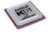
... Information AMD-K6®-2 Processor Data Sheet 21 Ordering Information Standard AMD-K6®-2 Processor Model 8 Products AMD standard products are available in volume for this device. Valid Ordering Part Number Combinations OPN Package Type Operating Voltage Case Temperature AMD-K6-2/550AGR 321-pin CPGA 2.2V-2.4V (Core) 3.135V-3.6V (I/O) 0°C - 70°C AMD-K6-2/533AFX 321-pin CPGA 2.1V-2.3V (Core) 3.135V-3.6V (I/O) 0°C - 65°C AMD-K6-2/500AFX 321...
... Information AMD-K6®-2 Processor Data Sheet 21 Ordering Information Standard AMD-K6®-2 Processor Model 8 Products AMD standard products are available in volume for this device. Valid Ordering Part Number Combinations OPN Package Type Operating Voltage Case Temperature AMD-K6-2/550AGR 321-pin CPGA 2.2V-2.4V (Core) 3.135V-3.6V (I/O) 0°C - 70°C AMD-K6-2/533AFX 321-pin CPGA 2.1V-2.3V (Core) 3.135V-3.6V (I/O) 0°C - 65°C AMD-K6-2/500AFX 321...

